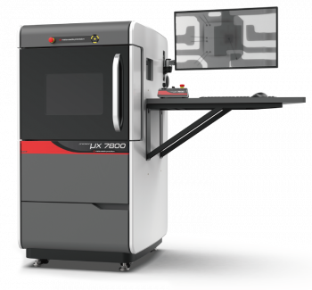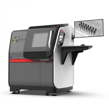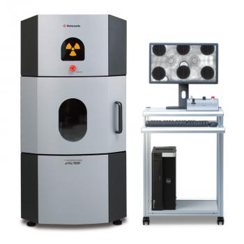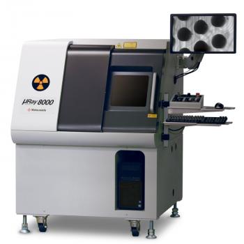


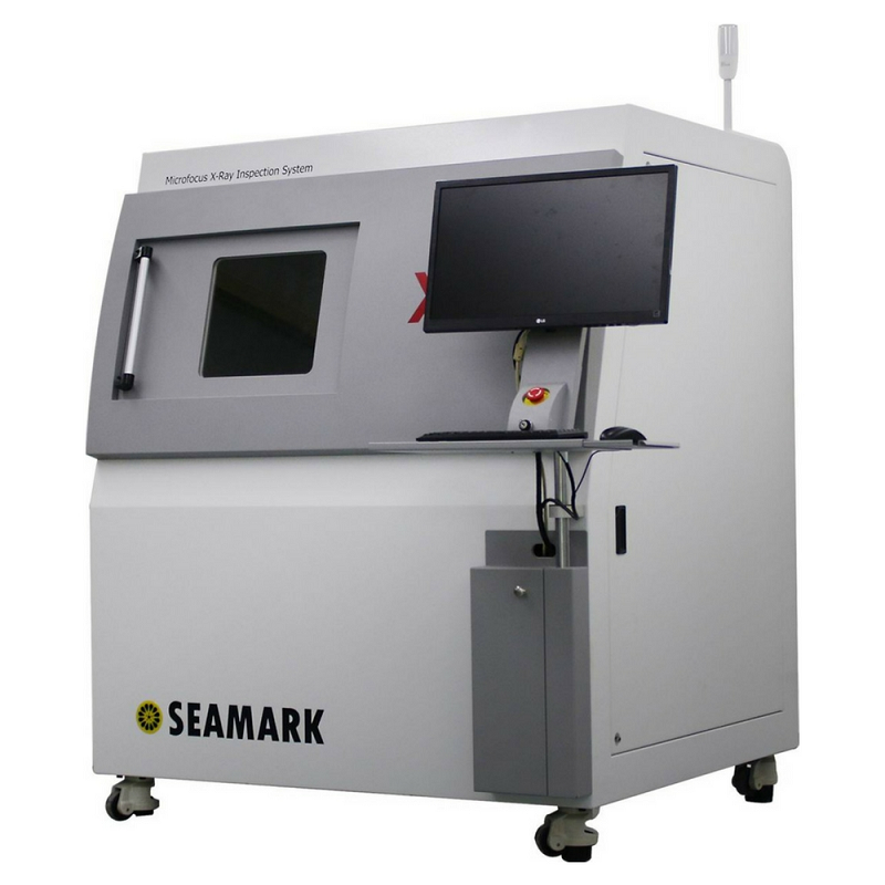
X6600 X-Ray Inspection Machine for Semiconductor, Packing components for Semiconductor, Packing components
A Leader in the Intelligent X-Ray Inspection Machine
X6600 X-Ray Inspection Machine Application Field
LED, SMT, BGA, CSP, Flip Chip Inspection
Semiconductor, Packing components
Battery Industry
Electronic components, Auto parts, Photovoltaic Industry
Aluminum Die Casting, Moulding Plastic
Ceramics, Other special Industries
Detection of high-definition video: joints open,short,bubbles and other defects at a glance
- 90KV 15 um closed X-ray tube,with long life,maintenance in free
- 1.3million high resolution digital flat panel detector
- Color image navigation
- Automatic programming detection and automatic analysis Not good or Pass
- More modular panels observation point setting
Stage Control Parts
- By the space bar to adjust stage speed: Slow, Constant and Fast
- Keyboard control X, Y, Z axis motion and the inclined angle
- User can detect the samples automatically by programmed
- Large navigation window, the image is very clear, mouse clicks will move the stage to a position that you need
NC programming
- A simple mouse clicks will create a Testing procedures
- The stage can be X, Y axis positioning; X-ray tube and the detector will be positioning in Z axis
- Software setting voltage and current
- Image setting: Brightness, contrast, automatic gain and exposure
- User can set the program switch pause time
- The anti-collision system can meet the maximum tilt and observe objects
- Automatic analysis BGA diameter, Void ratio, size and roundness
X6600 X-Ray Inspection Machine Youtube Demo: X-Ray Images Machine for Semiconductor, Packing components
X6600 X-Ray Inspection Machine Application:
- 1) Defect inspection in IC encapsulation, e.g.: layer separation, cracking, void, and line integrity.
- 2) Measuring chip size, measuring line curvature, measuring the proportion of solder area of components.
- 3) Possible defects in PCB manufacturing processes, e.g.: misalignment, solder bridge and open.
- 4) SMT solder short, cold solder, component shifted, solder insufficient, solder void inspection and measurement.
- 5) Defect inspection of open, short or abnormal connections that may occur in automotive wiring harnesses and connectors.
- 6) Inner rupture or hollow inspection in plastic or metal.
- 7) Battery stacking uniformity, electrode welding inspection.
- 8) Seed, biological material inspection etc.
- 9) Inspection of internal cracks and Defects analysis of internal conditions

BGA Image

PCB Board Image

IC Chip Image
INTRODUCTION VIDEO of X6600