
Advantages of the CMOS sensor in the GNR OES analyzer
14:22 - 27/01/2021
GNR Srl founded in 1984 is the world's leading manufacturer of OES emission spectroscopy analyzers. The company has a full range of solutions with traditional PMT technology, CCD technology and advanced CMOS technology. In this article let's explore the advantages of CMOS technology.
Analysis of Aluminum ADC12, ADC6 According to JIS H 5302 Standard
Main Magnesium Alloys used in Industrial Production
What is X-Ray Diffraction (XRD)
Handheld XRF for Positive material identification
GNR Srl was established in 1984 and is known to be one of the most experienced firms in the research, development and manufacture of Optical Emission Spectrometer (OES) in the world.
They took over OPTICA srl, one of the first and most famous European companies in the field of analytical equipment. Continued effort maintained over the years of operation has allowed GNR to rise to prominence among the most important Arc Emission Spectrophotometer manufacturers - with a 7% share worldwide.
One of the most important main components of an Optical Emission Spectrophotometer is the detector, which determines the ability of the alloy to detect the elements, the accuracy, the stability of the differential. chemical composition. And this component is also constantly being improved, we take a look at 3 technologies that have been used up to now:
PhotoMultiplier Tubes (PMT)
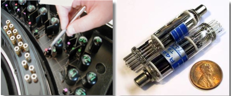
The first sensors to use were the Analog PhotoMultiplier Tubes, which is traditionally used and is still used in a number of applications at present due to its lower detection limit (LOD).
However, PMT technology is limited due to its very high cost, more complicated installation and more maintenance. It is also very difficult and expensive to upgrade or repair.
Charged Coupled Device (CCD technology)
CCD type sensors, which have been in use for more than 20 years, are digital, generally have higher LOD but are flexible and much cheaper. A CCD sensor does not capture a single wavelength, but rather a range of wavelengths.
To put it simply, we can imagine that today's digital cameras have evolved so much that they produce very fast and beautiful pictures that makes people forget about expensive, bulky mechanical cameras. The CCD sensor, too, has been continuously improved to better detect low wavelength elements (UV region), improving LOD, stability and accuracy compared to PMT sensor. It can be said that emission spectrophotometers equipped with CCD sensors can meet more than 90% of the general market demand.
CMOS – the newest technology
Main advantages are related to:
- Stronger Signal > Better Performance
- Improved ratio Signal / Ni
- No Blooming Effect
- Integration time reduced
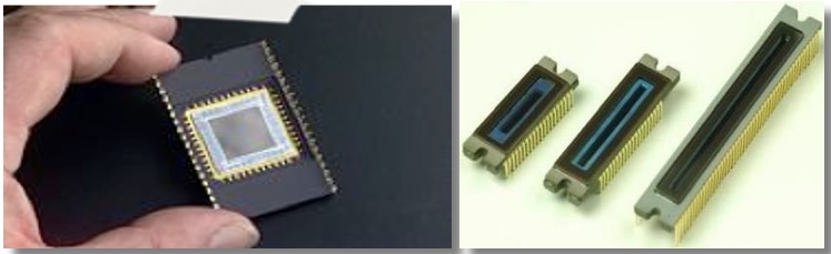
High sensitivity, photosensitive area with vertically long pixels
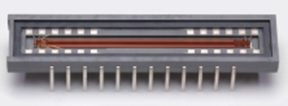
The detector identified is a high sensitivity CMOS linear image sensor using a photosensitive area with minute pixels. It has a long photosensitive area consisting of 4096 pixels, each with a pixel size of 7 x 200 µm.
Other features include high sensitivity and high resistance in the UV region.
It operates from a single 5 V supply making it suitable for use in spectrometers.
CMOS Linear Image Sensor: Comparison of Photosensitivity
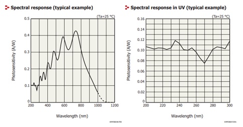
Photosensitivity 4 times better than previous component.
Photosensitivity 0.10 A/W till 130 nm that allow to measure also lines in VUV region
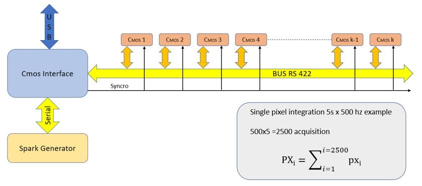
Actual CCD Electronic:
- Single Acquisition integration loop - 25ms: every 25 ms single px acquisition and digital integration
- No spark synchronization: acquisition in free running loop
- Number acquisition is independent from spark frequency (about 40 acquisition for second)
- Impossibility to gate the acquisition for trace analysis
New CMOS Electronic:

- Acquisition synchronized with spark
- Acquisition loop depend from spark frequency: 500 Hz mean 1 acquisition every 2ms; 500 acquisition/sec
- Lower time acquisition loop = 1ms (1000 Hz) [Max rate]
- Every spark system read the pixel and digitally integrate the value
- Due to fact that acquisition system is able to read single spark, in near future will be possible to implement gating procedure to improve LOD for critical element (Time Resolved Spectroscopy)
Comparison CMOS vs. CCD:
Parameter | TCD1304Ap | S11639 | Note |
Spectral range | 320 – 1050nm | 170 – 1050nm | With coating the actual detector can work till 140 nm but with less quantum efficiency. The new detector without window can easily reach 100 nm with good quantum efficiency |
Photosensitivity | 160 V/(lx*s) | 1300 V/(lx*s) | New detector is at least 10 times more sensible. |
Clock pulse frequency | Max 4Mhz | Max 10Mhz | New detector acquisition is at least 2 times faster. |
Blooming effect | Present | Not Present | This is very important parameter. New detector isn’t affected by blooming effect problem. This mean that is possible to detect line also where now we have saturation. |
Comparison between CCD and CMOS in saturation:
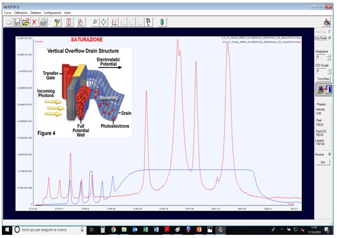
Same spectra of the previous slide but introducing spectral background function.
Antiblooming is really important when brightness range spans many order of magnitude like when we measure spectrochemical line. Electronic to prevent blooming involves some reduction in sensor performance especially for very low level light intensity.
P 1783 comparison: CMOS vs. CCD:
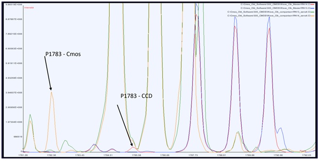
Using same spark conditions is possible to evaluate the difference between CMOS and CCD detector.
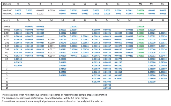
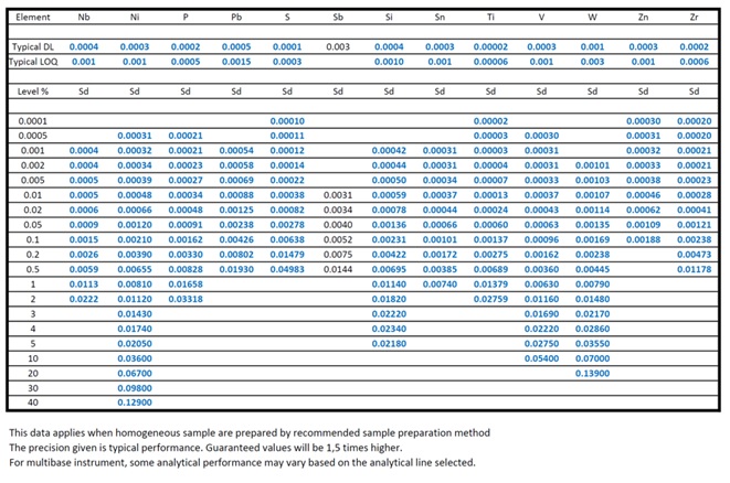
Typical Precision with S3 MiniLab 300 – Fe Matrix 1/2:
Through the above comparisons, we can see the great advantages of the latest generation CMOS sensor. With 37 years of experience in researching, developing and integrating digital sensors into the OES spectrum analyzer system, GNR aims to apply CMOS technology on all emission spectroscopy models, replacing not only CCD sensor but even PMT technology.
For more specific advice, please contact us!